Cybersquare
This document is given as though you personally requested it from me.
Vol. 30, No. 9: SEPTEMBER 1997, pp. 37-39
Will Physical Scalability Sabotage Performance Gains?
![[PDF ICON]](../images/pdficon.gif)
Doug Matzke Texas Instruments
Although reduced feature size is
good news in some respects, other factors will soon influence how we
wring performance from tighter integration. Wire scaling and its
interaction with faster clocks will restrict the performance increases
we've come to expect.
Many designers expect processor
performance to keep improving at the current rate indefinitely as
feature sizes shrink. However, as wire delays become a larger percentage
of overall signal delay and as clock speeds grow faster than transistor
speed, I believe performance increases will ultimately fall off. These
delays are inevitable simply because wires are not keeping pace with the
scaling of other features. In fact, for CMOS processes below 0.25
micron, the physical limits of wire scaling
1 may begin to change high-speed processor
design. That is, an unacceptably small percentage of the die will be
reachable during a single clock cycle.
To support my prediction, I have mapped trends in a metric
that relates time and distance and projections in clock speed across
eight processor generations, from 0.6 to 0.06  m. During this span
(probably 0.1 m)
we'll see a billion transistor processor. To illustrate how physical
scalability could affect the design of processors on this scale, I also
compared signal drive distance and clock speed for the span endpoints,
0.6 and 0.06 m.
m. During this span
(probably 0.1 m)
we'll see a billion transistor processor. To illustrate how physical
scalability could affect the design of processors on this scale, I also
compared signal drive distance and clock speed for the span endpoints,
0.6 and 0.06 m.
WIRE DELAY TRENDS
Wires do not scale well because the spacing
between them, the wire pitch, must continue to shrink so that
wires can connect to smaller transistors. As processes improve, and
on-chip wire cross-sections shrink, wire delays will increase per unit
length of wire (resistance is inversely proportional to the
cross-section of a wire). Making wires "taller" (vertically thicker) can
compensate, but eventually this approach fails because capacitance
between the sides of the wires and the substrate will also increase.
1
The final optimal aspect ratio is about 2
(vertical thickness/width), which means parallel wires would look like a
set of long 2 × 4's resting on their narrow sides with their
centers spaced by the pitch distance.Time-distance relationships
To see why wire delays are increasing, you
have to understand the relationship between a time scale and the
corresponding signaling distance. This may sound strange to some
engineers who have traditionally viewed connections as ideal, but the
community of computational scientists and physicists researching how
physical principles apply to computation has firmly established that
relationships exist between distance and time metrics.
2
For example, Patrick Bosshart of Texas Instruments has defined a scalable
metric that relates the wire time constant and signaling
distance. The wire time constant, or resistance-capacitance
(RC) time constant, is the overall propagation delay along a
section of wire, which is approximately the wire section's lumped
resistance times its lumped capacitance. Bosshart's metric is based on
an individual gate delay but also relates to the clock cycle because it
includes the number of gate delays per clock.Bosshart derived his metric using a design
rule of thumb typically applied at Texas Instruments: When gate and wire
delays match, signal propagation speed is optimal. This rule implies
that designers should insert a buffer gate when the RC time constant of
a length of wire equals the intrinsic gate delay. Under these
conditions, the distance from one buffer to the next the signal drive
distanceoccurs
in one gate delay's worth of time. This distance in turn defines a
signal drive region, a square area in which one side equals the
signal drive distance. This region is occupied by the number of gates a
particular signal can directly reach in a single gate delay without
using a buffer.
the signal drive
distanceoccurs
in one gate delay's worth of time. This distance in turn defines a
signal drive region, a square area in which one side equals the
signal drive distance. This region is occupied by the number of gates a
particular signal can directly reach in a single gate delay without
using a buffer.Assuming wire
technology stays the same, for a fixed RC time constant, the thinner
wires of advanced process technology must decrease in length. At the
same time, gate delay will decrease (the transistors that form gates
will become faster). Thus, the signal drive distance should decrease by
a faster-than-linear rate because it is the product of these two
factors. This means that the distance and number of gates directly
reachable by a signal in a single gate delay is shrinking faster than
the linear evolution of the CMOS process.Scalability projections
The results from Bosshart's SPICE modeling
support this. On a 0.6-m process with a typical gate delay of 250 ps, the equivalent
RC time constant represents a 5-mm length of wirealmost a third the
side of a 16-mm × 16-mm die.You can extrapolate these metrics to future processes, making
two reasonable assumptions:
- Gate delays will improve by
150 percent per process generation. The gate delay for the
0.06-m process
would thus be 15.6 psabout 16 times faster than with the 0.6-m process. The
associated signal drive distance metric will be 160 times shorter
(computed as the product of 10× wire scaling and 16×
transistor speed scaling). Therefore the wire length represented would
be 0.03125 mm (5 mm/160).
- Wire technology will improve 20
percent per process generation. The signal drive distance would
thus be four times longer, or 0.125 mm. This distance is still so small,
that a signal traveling across a future die size of 32 mm on a side
(assuming 10 percent increase in length per generation) would require
256 buffer gates.
To
calculate the number of reachable gates, I assume this future die
contains about 400 million gates (using the size forecast described
later). The signal drive region would contain the number of gates equal
to the total gates on a die times the ratio of the signal drive area to
the total die area. For the more advanced, 0.06-m technology, this would
be only 6,000 gates versus 100,000 for the 0.6-m process.This exercise illustrates that the number of
gates considered "local" to an unbuffered gate is shrinking, and more
buffers will be needed just to implement a design. Architectures that
cannot adapt to this constraint will become extinct. Even if wire
technology improvesand I'm not saying it won'tthe signal drive region would still shrink
because transistor speeds are improving faster than the linear process
evolution.
CLOCK SPEED TRENDS
Computers have historically improved
performance by 2× every 18 months or sothe infamous Moore's
law. During the 1980s, many performance gains came from integration
because we could squeeze larger systems onto a single chip. But chip
process improvements and integration alone can no longer improve
performance at a rate consistent with Moore's law. Performance
improvements must come from some resource, just as we extract a resource
like oil. Once we've exhausted the gushers of single-chip integration,
we must turn to more sophisticated techniques for extracting
performance, such as fast clocks and complex architectures. It's the
only way we'll stay on the performance curve that every competitor is
targeting. This do-or-die attitude is ingrained in both the processor
supplier and consumer cultures.
Clock speeds are improving at an accelerated rate because that's the
next easiest way to tap the performance well. The thinking goes
something like this: If we increase clock speed faster than improvements
in gate speed, we can just reduce the gates per clock and add more
pipeline stages. Unfortunately, the limit for aggressive frequency
design is most likely reached around four to five "complex" gates per
clock, or when basic adders are pipelined,
3 at which time the clock rate will improve
no faster than gate speed or circuit improvements. But let's be conservative for the sake of
argument, and assume a constant 25 simple gate delays per clock cycle.
The maximum clock frequency for the 0.6-m process would then be 166 MHz and, for the 0.06
m, 2.5 GHz.
Because time and distance are
related, the number of gate delays per clock also dictates how far a
signal can propagate before you must insert a synchronization register.
Assuming roughly half the 25 gate delays are related to wire delays, the
processor can traverse 12 signal drive distances in a clock period.
Bosshart also developed this metric, which I call the clock locality
metric. For processes above 0.18 m, the entire die can be reached in a clock
cycle, but at 0.06 m, a signal can traverse only 1.5 mm (12 × 0.125 mm).
To move a signal farther, the designer must add a pipeline register to
resynchronize the signal to a local version of the clock. Long distance
travel on a die requires inserting both buffers and registers.
Thus, as
Figure 1
shows, the percentage
of the die that can be reached within a few clock cycles is decreasing
at an alarming rate; faster clocks would only accelerate this effect.
For a 0.06-m
process (lower right), for example, a signal can reach only five percent
of the die's length in a clock cycle. Because the clock is also bounded
by this restriction, the effective clock wavelength is much shorter than
the die length.
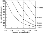
Figure 1. Trends for the clock locality metric. Dashed line marks
the generation (0.1 m) at which a billion transistor processor will first occur.
At that point, only 16 percent of the die will be reachable within a
single clock cycle.
This metric makes the wire scaling problem understandable in
terms of the number of clocks required to access a remote part of the
die. Essentially this distance segregates an integrated chip into little
isolated islands of logic, and it is impossible to build superhighways
to improve this delay. Therefore, commonly used architectural elements
(like register files and crossbar switches) that increase size
nonlinearly with complexity will not scale well on more advanced
processes with slower wires and faster clocks.
REACHING A BILLION
TRANSISTORS
So how
do these metrics translate into design parameters for billion-transistor
processors? Assuming a million gate capacity at 0.6 m, the 0.06-m process would contain
400 million gates (100 times more gates, four times bigger). If this die
consisted entirely of four-transistor logic gates, it would represent
the first billion transistor processor. Most likely, SRAM (with many
more smaller transistors) for on-chip caches will occupy over half the
die area. This means that the first billion transistor processor is
likely to appear in a 0.1-m process, as the dashed vertical line in
Figure 1 indicates.
The figure also shows that in the 0.1-m process, only 16
percent of the die length is reachable within one clock period (at 1.2
GHz). Each clock region contains two million gates, so eight
synchronizing pipeline registers are needed for the signal to propagate
across the entire die length. The signal drive distance that an
unbuffered gate can directly reach would be 0.36 mm, which will
constrain the design into small regions of approximately 13,000
gates.
CONCLUSION
Shrinking signal drive distance
and clock locality metric indicate that an ever-increasing grain size
for complex architectures
4 cannot continue. Large architectures with
good locality and corresponding floor planning will survive; other large
architectures will give way to finer grained architectures
5 that scale well with poor wires. The
individual smaller regions of logic or memory in future large designs
will be distributed over the die, making a locality metric between these
regions more important. Architectures that require long-distance, rapid
interaction will not scale well, since propagation latency would be
measured in tens of clocks cycles. Fast clocks with wavelengths much
shorter than the die size will compound clock skew and synchronization
problems.
References
1. M. Bohr, "Interconnect ScalingThe Real Limiter to
High Performance ULSI," Proc. Int'l Electron Devices
Meeting, IEEE Press, New York, 1995, pp. 241-244.
2. D.
Hillis, "New Computer Architectures and Their
Relationship to Physics or Why Computer Science is No Good,"
Int'l J. Theoretical Physics, Vol. 21, Nos. 3, 4, 1982, pp.
255-262.
3. C. Lemonds, "A 500 MHz,
One Volt, 16 by 16 Multiplier for DSP Cores," Proc. VLSI
Signal Processing Workshop, IEEE Press, New York, 1996, pp.
481-484.
4. F. Preparata, "Horizons
of Parallel Computation," Tech. Report CS-93-20, Brown
University, Providence, R.I.
5. W. Dally, "A
Universal Parallel Computer Architecture," New Generation
Computing, Vol. 11, 1993, pp. 227-249.
Doug Matzke is a senior
member of the technical staff in the Digital Signal Processing group at
Texas Instruments. His research interests include the limits of
computing, fast cycle-based simulators, and design tools.Matzke received a BSEE from the
University of Wisconsin-Madison and an MSEE from the University of
Texas. He is a member of the IEEE and ACM. Contact him at;

